Intel, the world’s largest chip maker recently announced about the CPU architecture “Lakefield” which is built upon Intel’s Sunny Cove microarchitecture with AI and Crypto Acceleration. Sunny Cove is designed to increase performance per clock and power efficiency for general purpose computing tasks. It enables reduced latency and high throughput, as well as offers much greater parallelism which is expected to improve experiences from gaming to media to data-centric applications.
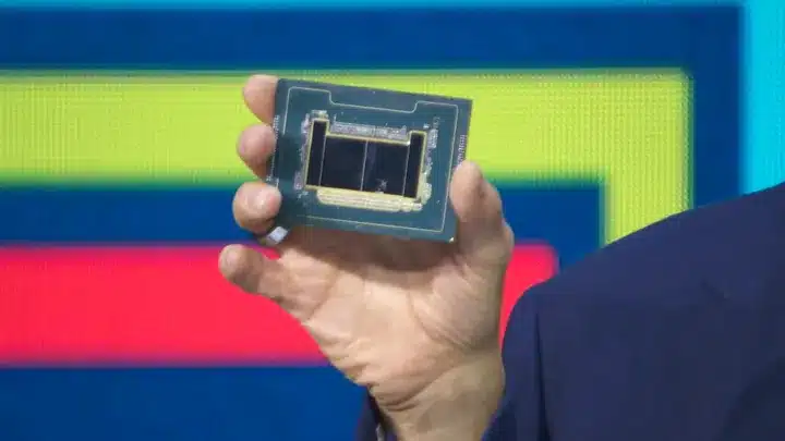
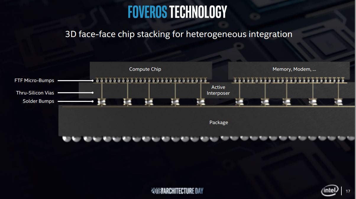
The technical strategy of the hybrid CPU architecture enables a combination of different CPU core architectures on a single product such as the processor has 5 cores combining one 10nm Sunny Cove core with four 10nm-based small core. Hence, it results in power efficiency, immersive graphics, I/O and memory within the 12nm hybrid CPU architecture. Then the hybrid CPU architecture is packaged in 3D packaging technique known as Foveros where different pieces of IP together are stacked in 3 dimensions instead of 2D.
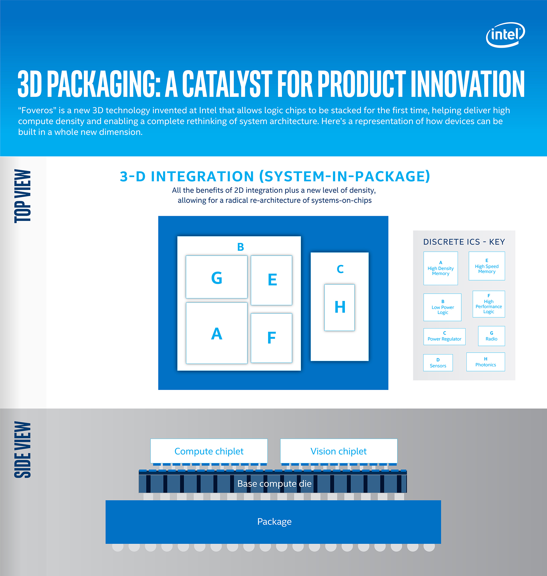
According to this journal, the chip maker demoed a design built with FOVEROS. It was an x86 design combining a large Sunny Cove X86 core with four smaller Atom cores, all on one 10nm device, to form a hybrid x86 CPU. It had one Sunny Cove core with 0.5 MB of private medium-level cache, and four Atom cores with a shared 1.5 MB L2 cache. Then there is an “Uncore” that contains 4MB of last-level cache, a quad-channel 4×16-bit memory controller supporting LPDDR4, a Gen11 graphics controller, a Gen 11.5 display controller, an imaging IPU, and MIPI with DisplayPort 1.4. On top of that was package-on-package (PoP) memory.
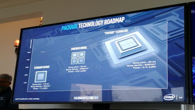
Intel’s chief architect, Raja Koduri is one of the masterminds behind this 3D stacking technology. Foveros is a 3D packaging technology which brings the benefits of 3D stacking to enable logic-on-logic integration. It paves the way for devices and systems combining high-performance, high-density, and low-power silicon process technologies and is expected to extend die stacking beyond traditional passive interposers and stacked memory to high-performance CPU, graphics and processors.
The first Foveros product will combine a high-performance 10nm compute-stacked chiplet with a low-power 22FFL base die. It will enable the combination of world-class performance and power efficiency in a small form factor and it also enables the combination of world-class performance and power efficiency in a small form factor. According to reports, Intel says that Foveros products will be shipping in the second half of 2019 and that the technology is ready for mass-market production—not just specialized or customized processors, but mainstream CPUs.
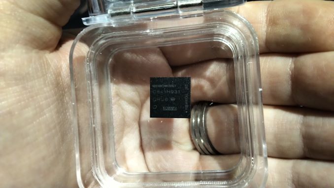
Lakefield, built with Foveros
According to this report, Ramune Nagisetty, Director of Intel’s Process and Product Integration said that when dies are stacked that known good dies (i.e. those that pass yield tests) are used, which requires bare die testing before assembly. Some of Intel’s previous development processes have needed to be adjusted in order to assist for technologies like Foveros and products like Lakefield, as well as other products in the future. She further added that Intel has not specifically looked into advanced cooling methods for Foveros type chips, but did expect work in this field over the coming years, either internally or externally.
Perks Of This Technology
This technology helps in manufacturing smaller chips which result in manufacturing smaller boards in more efficient and better design which will unleash greater performance of platform innovation in the industry as well as innovative devices.
- Advanced manufacturing processes and packaging
- Super-fast memory
- Interconnects
- Embedded security features
Importance In Machine Learning
In the current scenario, two classes of chip designs are being used which is Graphics Processing Unit (GPU) and Field Programmable Gate Array(FPGA). GPU has been portraying a very crucial role in the field of deep learning such as Convolution Neural Network (CNN), Recurrent Neural Network (RNN), etc. While the reprogramming feature of FPGA makes it more usable in the machine learning industry. The chipsets are thus helping the organisations to get impact on more machine learning technologies.